
One-stop PCB Production
From start to finish, our industry experts will be with you. Start your journey with us.


Production Process
-
“Design Review and Tool Preparation”:
Customer-supplied data (Gerber) is used to generate manufacturing data for the specific PCB. We review the Gerber files and, after completing the inspection, prepare the necessary data for production.
Once confirmed, the data is sent to the factory, and the base material is cut into working panel sizes.
-
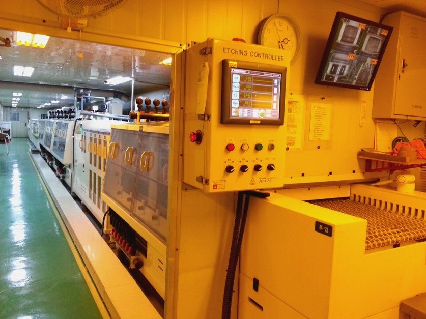
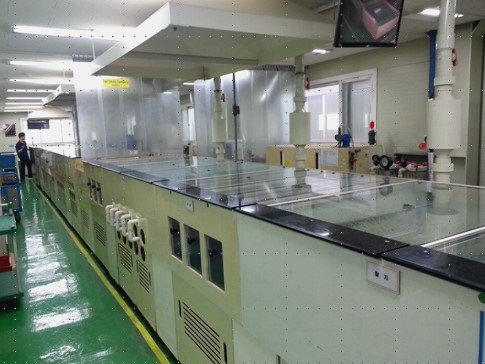
“Inner Layers Imaging”:
This process transfers electronic data to the PCB surface using photosensitive dry-film and exposure to UV light.
Steps: Pre-treatment -> Laminating -> Exposure -> Developing -> Etching -> Stripping
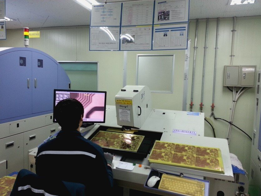
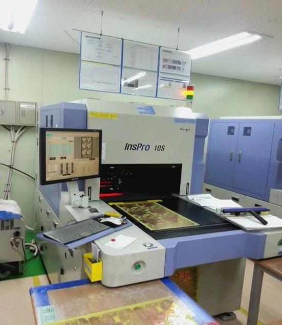
“AOI (Automated Optical Inspection)”:
An inspection process where the circuitry is compared against digital images to verify that the design is accurate and free of defects.
“Lay-up and Bond (Lamination)”:
Under controlled heat and pressure, the inner layer core, copper foil, and prepreg are bonded to create a solid, rigid stack-up.
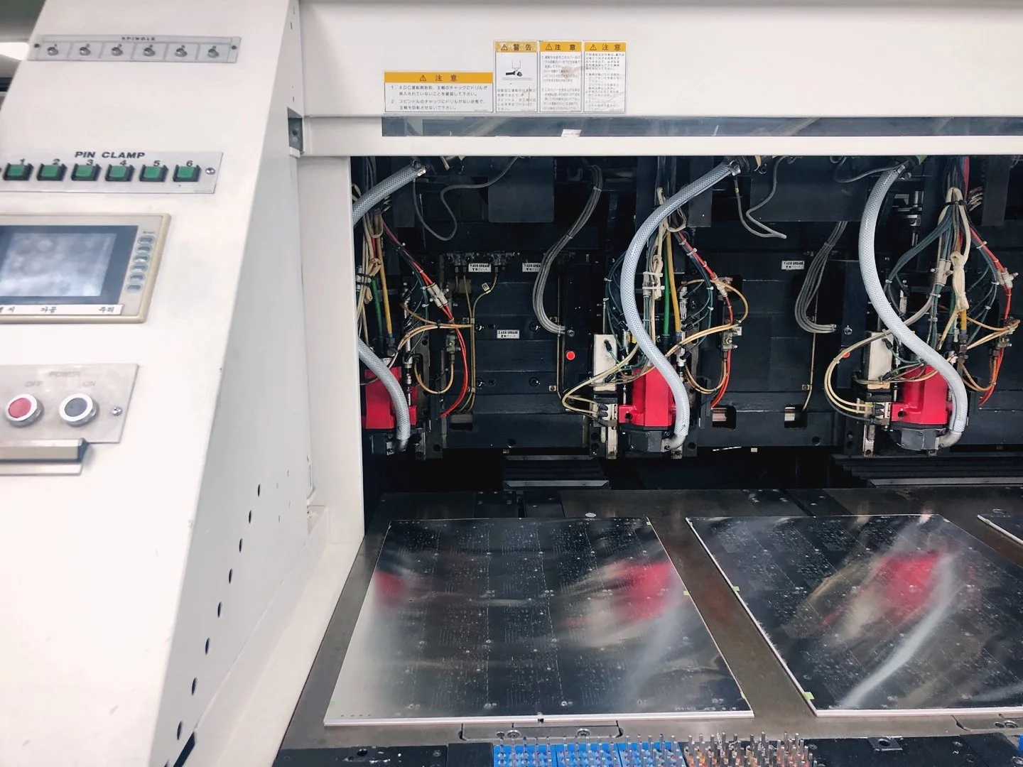
“Drilling”:
Holes are drilled into the PCB to facilitate electrical connections. Clean and precise drilling ensures high-quality copper plating and effective hole connections.
“Copper Plating (Cu Plating)”:
Chemical deposition of copper onto the hole walls creates electrical connections between the drilled holes and all PCB layers.
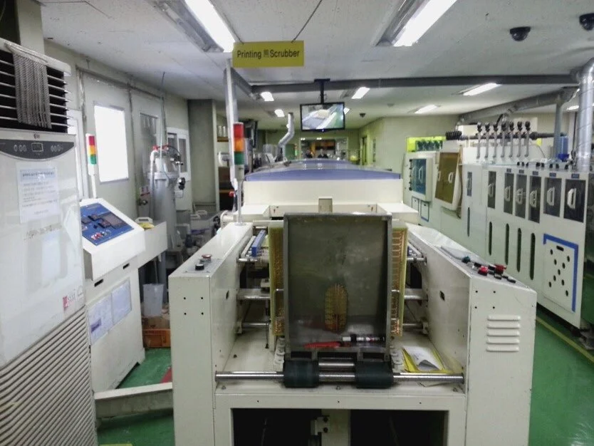
“Outer Layer Imaging”:
Similar to the inner layer process, the outer layer undergoes:
Steps: Pre-treatment -> Laminating -> Exposure -> Developing -> Etching -> Stripping
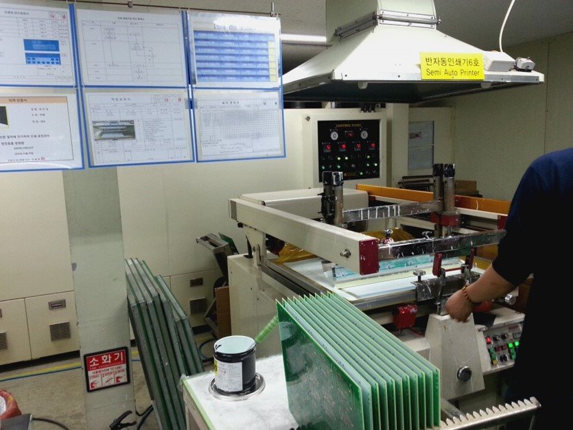
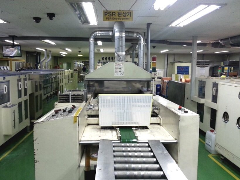
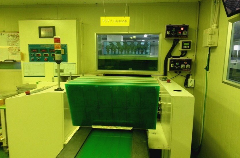
“PSR (Solder Mask)”:
A solder mask is applied to the PCB surface to protect areas from soldering and prevent shorts.
“Surface Treatment”:
A variety of surface finishes are applied to exposed copper areas, ensuring solderability and protection from corrosion.
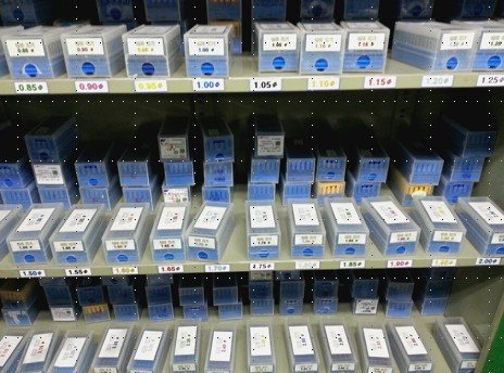
Common finishes include: HASL, LF-HASL, ENIG, OSP, Immersion Silver, Immersion Tin, ENEPIG
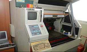
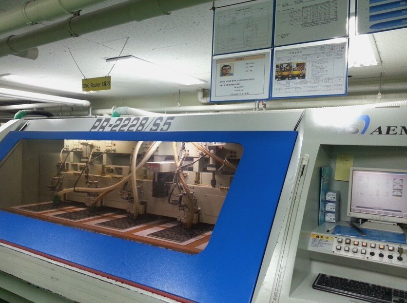
“Profiling”:
The PCB panels are machined to specific sizes and shapes according to the customer’s design. Options include:
V-scoring
Routing
“Electrical Test (BBT)”:
The PCB panels are machined to specific sizes and shapes according to the customer’s design. Test methods available:
Universal Test
Flying Probe
-
“Final Inspection, Packing & Delivery, and After-sales Service”
Once the board has passed the final inspection, it is packed securely for delivery. We also provide after-sales service to ensure customer satisfaction.